- 您现在的位置:买卖IC网 > Sheet目录1917 > DSPIC30F3013-20I/ML (Microchip Technology)IC DSPIC MCU/DSP 24K 44QFN
PIC18F46J11 FAMILY
DS39932D-page 152
2011 Microchip Technology Inc.
10.7.3.2
Output Mapping
In contrast to inputs, the outputs of the PPS options are
mapped on the basis of the pin. In this case, a control
register associated with a particular pin dictates the
peripheral output to be mapped. The RPORx registers
are used to control output mapping. The value of the bit
field corresponds to one of the peripherals and that
peripheral’s output is mapped to the pin (see Table 10-
14).
Because of the mapping technique, the list of
peripherals for output mapping also includes a null
value of ‘00000’. This permits any given pin to remain
disconnected from the output of any of the pin
selectable peripherals.
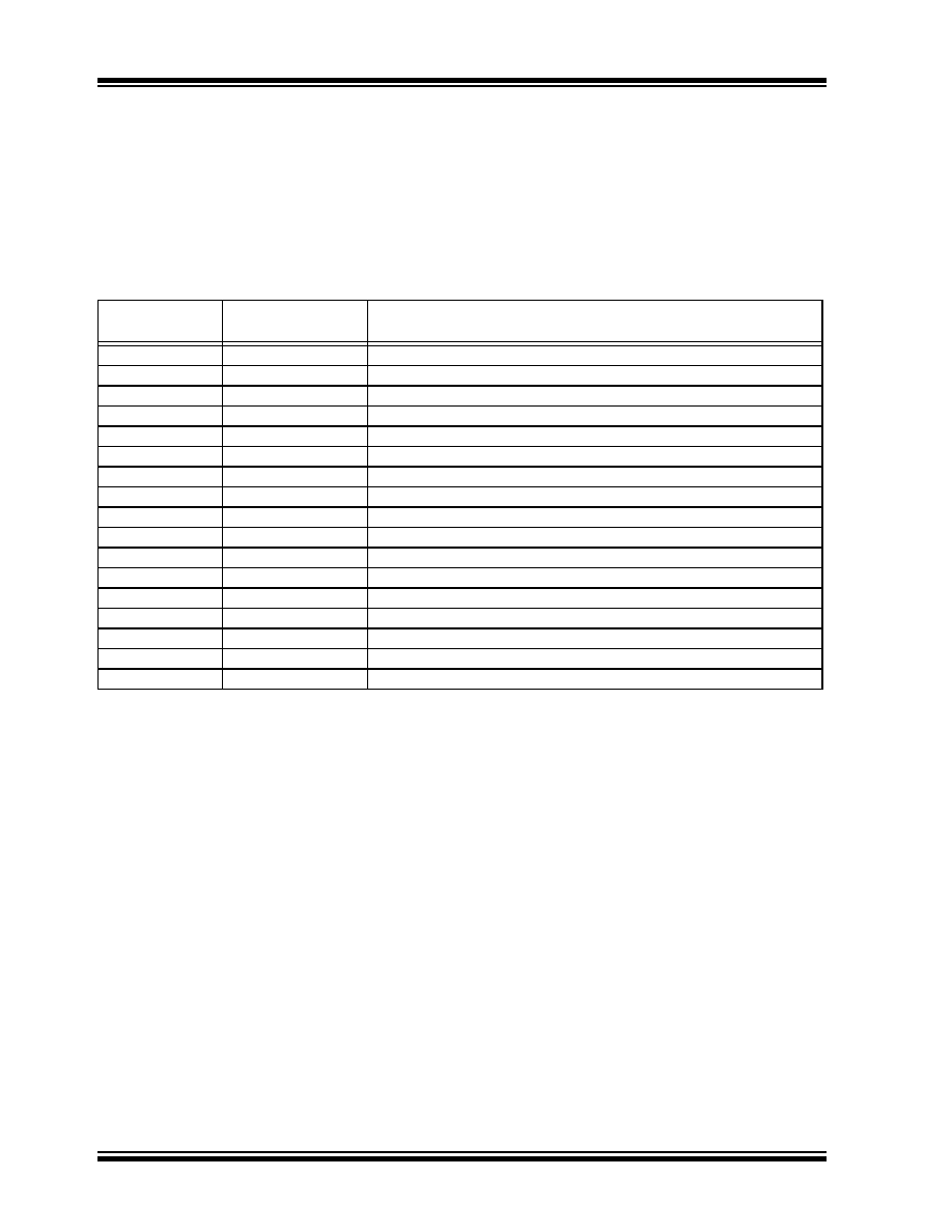
TABLE 10-14: SELECTABLE OUTPUT SOURCES (MAPS FUNCTION TO OUTPUT)
Function
Output Function
Number(1)
Output Name
NULL
0
NULL(2)
C1OUT
1
Comparator 1 Output
C2OUT
2
Comparator 2 Output
TX2/CK2
5
EUSART2 Asynchronous Transmit/Asynchronous Clock Output
DT2
6
EUSART2 Synchronous Transmit
SDO2
9
SPI2 Data Output
SCK2
10
SPI2 Clock Output
SSDMA
12
SPI DMA Slave Select
ULPOUT
13
Ultra Low-Power Wake-up Event
CCP1/P1A
14
ECCP1 Compare or PWM Output Channel A
P1B
15
ECCP1 Enhanced PWM Output, Channel B
P1C
16
ECCP1 Enhanced PWM Output, Channel C
P1D
17
ECCP1 Enhanced PWM Output, Channel D
CCP2/P2A
18
ECCP2 Compare or PWM Output
P2B
19
ECCP2 Enhanced PWM Output, Channel B
P2C
20
ECCP2 Enhanced PWM Output, Channel C
P2D
21
ECCP2 Enhanced PWM Output, Channel D
Note 1:
Value assigned to the RPn<4:0> pins corresponds to the peripheral output function number.
2:
The NULL function is assigned to all RPn outputs at device Reset and disables the RPn output function.
发布紧急采购,3分钟左右您将得到回复。
相关PDF资料
DSPIC30F4011-30I/ML
IC DSPIC MCU/DSP 48K 44QFN
DSPIC30F4013-30I/ML
IC DSPIC MCU/DSP 48K 44QFN
DSPIC30F5013-30I/PT
IC DSPIC MCU/DSP 66K 80TQFP
DSPIC30F5015-30I/PT
IC DSPIC MCU/DSP 66K 64TQFP
DSPIC30F6010-20E/PF
IC DSPIC MCU/DSP 144K 80TQFP
DSPIC30F6010A-30I/PF
IC DSPIC MCU/DSP 144K 80TQFP
DSPIC30F6013A-30I/PF
IC DSPIC MCU/DSP 132K 80TQFP
DSPIC30F6014-30I/PF
IC DSPIC MCU/DSP 144K 80TQFP
相关代理商/技术参数
dsPIC30F3013-20I/SO
功能描述:数字信号处理器和控制器 - DSP, DSC 28LD 20MIPS 24 KB RoHS:否 制造商:Microchip Technology 核心:dsPIC 数据总线宽度:16 bit 程序存储器大小:16 KB 数据 RAM 大小:2 KB 最大时钟频率:40 MHz 可编程输入/输出端数量:35 定时器数量:3 设备每秒兆指令数:50 MIPs 工作电源电压:3.3 V 最大工作温度:+ 85 C 封装 / 箱体:TQFP-44 安装风格:SMD/SMT
dsPIC30F3013-20I/SP
功能描述:数字信号处理器和控制器 - DSP, DSC 28LD 20MIPS 24 KB RoHS:否 制造商:Microchip Technology 核心:dsPIC 数据总线宽度:16 bit 程序存储器大小:16 KB 数据 RAM 大小:2 KB 最大时钟频率:40 MHz 可编程输入/输出端数量:35 定时器数量:3 设备每秒兆指令数:50 MIPs 工作电源电压:3.3 V 最大工作温度:+ 85 C 封装 / 箱体:TQFP-44 安装风格:SMD/SMT
DSPIC30F3013-30I/ML
功能描述:数字信号处理器和控制器 - DSP, DSC Sensor RoHS:否 制造商:Microchip Technology 核心:dsPIC 数据总线宽度:16 bit 程序存储器大小:16 KB 数据 RAM 大小:2 KB 最大时钟频率:40 MHz 可编程输入/输出端数量:35 定时器数量:3 设备每秒兆指令数:50 MIPs 工作电源电压:3.3 V 最大工作温度:+ 85 C 封装 / 箱体:TQFP-44 安装风格:SMD/SMT
DSPIC30F3013-30I/SO
功能描述:数字信号处理器和控制器 - DSP, DSC Sensor RoHS:否 制造商:Microchip Technology 核心:dsPIC 数据总线宽度:16 bit 程序存储器大小:16 KB 数据 RAM 大小:2 KB 最大时钟频率:40 MHz 可编程输入/输出端数量:35 定时器数量:3 设备每秒兆指令数:50 MIPs 工作电源电压:3.3 V 最大工作温度:+ 85 C 封装 / 箱体:TQFP-44 安装风格:SMD/SMT
DSPIC30F3013-30I/SO
制造商:Microchip Technology Inc 功能描述:IC DSC 16BIT 24KB 40MHZ 5.5V SOIC-28
DSPIC30F3013-30I/SP
功能描述:数字信号处理器和控制器 - DSP, DSC Sensor RoHS:否 制造商:Microchip Technology 核心:dsPIC 数据总线宽度:16 bit 程序存储器大小:16 KB 数据 RAM 大小:2 KB 最大时钟频率:40 MHz 可编程输入/输出端数量:35 定时器数量:3 设备每秒兆指令数:50 MIPs 工作电源电压:3.3 V 最大工作温度:+ 85 C 封装 / 箱体:TQFP-44 安装风格:SMD/SMT
DSPIC30F3013-30I/SP
制造商:Microchip Technology Inc 功能描述:16-Bit Digital Signal Controller
dsPIC30F3013T-20E/ML
功能描述:数字信号处理器和控制器 - DSP, DSC 44LD 20MIPS 24 KB RoHS:否 制造商:Microchip Technology 核心:dsPIC 数据总线宽度:16 bit 程序存储器大小:16 KB 数据 RAM 大小:2 KB 最大时钟频率:40 MHz 可编程输入/输出端数量:35 定时器数量:3 设备每秒兆指令数:50 MIPs 工作电源电压:3.3 V 最大工作温度:+ 85 C 封装 / 箱体:TQFP-44 安装风格:SMD/SMT